Custom PWM Configuration for Arduino MKR WiFi 1010 (SAM based)
High-frequency PWM is a necessity for some applications, like flicker free video lighting and interfacing with certain types of 4-wire PWM controlled fans. This guide covers the basics of configuring and using the built in PWM generator of the Atmel SAM D21 micro-controller that’s used in certain Arduino devices, like the MKR WIFI 1010.
The impetus for this project goes back to 2015 when I started looking into building a DiY LED lighting system for video and photography applications. At the time I my intent was to use the AVR based Arduino Uno and it’s PWM engine. However, I ran into issues flicker due to the relatively low PWM frequency.
At the time, I didn’t have an effective solution to this problem. Dimming LEDs can be done either by using a constant current power supply and controlling the current through the LEDs, or with pulse width modulation (PWM). Both of these methods have their trade-offs, with PWM being slightly easier to implement, as most micro controllers have PWM generators built in, but hash the downsize of strobing the lights.
I did know that PWM could be used, as there are LED systems that use it and don’t flicker, but I wasn’t completely clear on how they were accomplishing that. However, earlier this year when looking into LEDs for bias lighting my workstation, I ran across an article by Waveform Lighting, that talked about using a 25 KHz PWM frequency to produce flicker free lighting for video use.
Simultaneously, as part of the bias lighting project, I also started working with the Arduino MKR WiFi 1010. As it was an inexpensive way to get a Wi-Fi network enabled device to control my lighting system. This way I could integrate it into my home automation/light control system and control the bias lights from my computer, such as turning them on with the computer.
This applies to most if not all current SAM D21 based Arduinos including:
- Arduino Zero
- Arudino MKR Fox
- Arduino MKR 1000
- Arduino MKR WiFi 1010
- Arduino MKR GSM 1400
- Arduino MKR WAN 1300
- Arduino MKR Zero
The code presented in this article was testing on a MKR WiFi 1010 and compiled using version 1.8.8 of the Arduino development environment.
Calculating a PWM Frequency and Resolution
When it comes to PWM, the biggest advantage that the SAM21 based Arduinos over the AVR ones is that they have a much faster clocks, as fast as 96 MHz, available to run the counters with. This allows for better PWM resolution while maintaining a high frequency.
For example, an AVR based Arduino Uno could do a 25 KHz PWM on it’s timer 1 output, and so with just over 9-bits worth of resolution. A SAM based Arduino can run at the same frequency but provide just under 11 bits of resolution using the 48 MHz clock, and just under 12 bits of resolution at 96 MHz.
In many applications the higher resolution isn’t that importantly. However, for photographic lighting, which was the project that got me started down this path, the resolution translates to a wider controllable range.
Generally speaking though, the PWM problem starts with knowing the PWM frequency and an a minimum resolution, and having to work backwards to to figure out the dividers that the system will use.
For this article I’ll be working with the single-slope PWM mode, as that’s what I’m using in LED light panel controller project. However, the methodology is the same for other PWM modes, only you’ll need to adjust the equations.
Single-slope PWM on the SAM21 is set’s its frequency by incrementing counter once every clock cycle counting from 0 to a user-defined TOP value. The output’s duty cycle is set by a second value (CCx) that is between 0 and TOP which toggles the output.
For example, a TOP of 255 would provide an 8-bit resolution PWM, with the CCx counter set to 127, the output would be driven high while the counter is between 0 and 127, then pulled low until the counter resets to 0. In this example, the PWM system would generate a duty cycle of 50%.
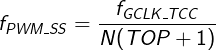
Pages 660 and 661 of the Atmel datasheet for the SAMD21 provides the following two equations for SSPWM.

The clock divider, N, in Equation 2, can be set to one of the following values: 1, 2, 4, 8, 16, 64, 256, and 1024.
Synchronization
One added complexity of the SAM based Arduinos is the need to synchronize registers between the various clock domains when changing them.
Not all registers need to be synchronized in all cases. Moreover, the results of not synchronizing them varies from subsystem to subsystem.
Further, the SAM uses two broad synchronization mechanisms. Some modules use a common synchronization scheme. In this scheme there is only a single sync bit covering all the registers. With these devices, the program must wait for synchronization to complete before it can move on to setting a value in another register.
The second method is a distributed synchronization scheme. Modules that use this configuration will have sync bits for each register, consequently, multiple registers can be written to before waiting for the synchronization to take place.
When it’s necessary to check synchronization, the code samples provided here will use a loop structure to poll the SYNCBUSY bit to halt further operations until the register is synchronized.
When operating at high frequencies, synchronization takes place in a reasonably short amount of time. According to the documentation the synchronization should take no less than 5 * PGCLK + 2 * PAPB and no more than 6 * PGCLK + 3 * PAPB. Where PGCLK is the period of the generic clock and PAPB is the period of the peripheral bus clock.
For example, configuring a write-sync register in the TCC module that’s operating with a GCLK of 48 MHz (~21 ns), and an APBC clock of 48 MHz (~21 ns), will take between 147 ns and 189 ns to sync.
While I wouldn’t necessarily recommend not waiting for synchronization to take place it may be safe to omit the synchronization waits when a register will not be written to for a sufficiently long time.
For example, my PWM controller implements a smooth dimming transition when changing duty cycles. This transition is achieved by updating the TCCx_CCBn register every ~10 ms. This is sufficiently longer than then <200 ns sycn time, that it may not be expressly necessary to wait for syncs before proceeding.
Configuring the Clock Source
The first part of configuring PWM on the SAM based Arduinos is to configure a clock source. The SAM D21 has 9 clock generators that can be configured. However, as best as I can tell from my research, the first 4 of these (0-3) are used by the Arduino environment, leaving 4-8 available for other purposes.
The clock generators on the SAM D21 can be driven from 7 different clock sources. Several of these run in the 32 KHz range, and aren’t especially interesting for this application. The OSX8M runs at 8 MHz, and the afore mentioned DFLL48M and FDPLL95M run at 48 and 48–96 MHz respectively. These 3 clocks are the most useful for the kind of high-frequency high-resolution operation that I’m after.
The GCLK controller primarily uses 3 registers for configuration. Though there are 9 clock, there aren’t separate control registers for each of them. Instead each register has an 3-bit ID field that is used to select the clock being modified in the operation.
The code that follows, shows the configuration to use the DFLL48M 48 MHz source. However, if you want to use another source the configuration is done by changing the GCLK_GENCTRL_SRC_DFLL48M constant another option in the following code sample. You can either use the Arduino defines or just set the binary values manually in from the chart on page 107 of the datasheet.
Generic Clocks 4-8 can further be scaled by an arbitrary division factor. Clocks 4-8 support a 16-bit unsigned value for this division factor providing a lot of flexibility for the ultimate clock speed.
The code samples in this article use a divisor of 1, so there’s no clock division, however changing the value in GCLK_GENDIV_DIV() will change the setting.
Setting up the a generic clock source is relatively straight forward.
- Initialize the Clock’s Division register
- Enable It
- Configure the Clock
// Set the divisor for GCLK5.
REG_GCLK_GENDIV = GCLK_GENDIV_DIV(1) |  // Set divisor to 1
                  GLCK_GENDIV_ID(5);  // For GCLK5
while(GCKL->STATUS.bit.SYNCBUSY);

// Set the clock source, duty cycle, and enable GCLK5
REG_GCLK_GENCTRL = GCLK_GENCTRL_SRC_DFLL48M |  // Set 48MHz source
                   GCLK_GENCTRL_IDC |          // Improve Duty Cycle
                   GCLK_GENCTRL_GENEN |        // Enable GCLK
                   GCLK_GENCTRL_ID(5);         // For GLCK5
while(GCLK->STATUS.bit.SYNCBUSY);

// Route GLCK5 to TCC0 & TCC1, and enable the clock.
REG_GCLK_CLKCTRL = GCLK_CLKCTRL_ID_TCC0_TCC1 | // Route GCLK5 to TCC0 & 1
                   GCLK_CLKCTRL_CLKEN |        // Enable the clock
                   GCLK_CLKCTRL_GEN_GCLK5;     // Select GCLK5
while(GCLK->STATUS.bit.SYNCBUSY); The first operation is to write to the GCLK_GENDIV register to configure the clock’s divider. GCLK_GENDIVis a 32-bit register where bits[23:8] are the division factor, and bits[3:0] are the address. In this instance, we’re initialization the division factor to 1 by writing a 1 to bit 8, for the clock set by the address 0101b in ID[3:0] respectively.
The clock configuration registers GENDIV and GENCTRL require synchronization on write. Because the GCLK controller uses a common synchronization mechanism after altering these registers, it’s necessary to wait for the STATUS.SYNCBUSY bit to clear before making further changes to the registers.
Changing a synchronized register in the GCLK module while the SYNCBUSY bit is set will stall the CPU until the operation has completed successfully. This will prevent the CPU from being able to handle interrupts while the synchronization is pending.
According to the SAM D21 documentation, the CLKCTRL register does not require synchronization when written to. However, I’ve included the synchronization instruction to err on the side of caution.
For the most part, waiting for synchronization when altering GCLK settings is not strictly necessary. Yes, the CPU will stall, but the operations will complete successfully. However, I would suggest it’s good practice to handle this properly in your code.
The second operation configures and enables the specific clock. For this operation we’re:
- Setting the clock source to DFLL48M by writing
0x07to theSRC[4:0]field (bits 8–14) - Enabling IDC by writing 1 to bit 17 (
IDC) - Enabling the clock itself by writing 1 to bit 16 (
GENEN) - and choosing the GCLK5 by writing the address 0x05 to
ID[3:0]to the first 4 bits.
Regarding IDC, the Atmel documentation says the following:
Bit 17 – IDC: Improve Duty Cycle
This bit is used to improve the duty cycle of the generic clock generator when odd division factors are used.
0: The generic clock generator duty cycle is not 50/50 for odd division factors.
1: The generic clock generator duty cycle is 50/50.
I’ve enabled IDC in this code in part because it’s usually recommended in the guides and examples I found when researching this. Moreover, as far as I can tell, there’s no actual harm in enabling it.
However, strictly speaking it’s not always necessary. In this case, because the clock is not being divided at all, there is no imbalance created by a division by an odd number. Moreover, in many applications it may not be important for the clock to have a 50/50 duty cycle, and a 49/51 duty cycle may be sufficient.
Also note, I chose clock 5 here for my device, with little rhyme or reason. Most demonstrations on line use clock ID 4. To select a different clock change the number in the GCLK_..._ID() field to reflect the clock you’re using. As I said before, clocks 0–3 are used by the Arduino environment, so you’ll want to pick clock 4 or higher.
The final step is to route the generated clock to the TCC module as the PWM generation signal. This is handled in the last 2 lines of code, where the CLKCTRL register is used to enable clock 5 and set the output to TCC0 and TCC1.
Output Pin Configuration
The SAM D21 MCUs provide a lot of internal flexibility in terms of being able to route signals around the chip and to the GPIO pins. In this instance we need to to configure the pins that we want to use for output and attach them to the Timer Counter for Control Applications (TCC) module.
This is the part I got most hung up on as it’s, in my opinion at least, the most confusing.
Lets start with the physical side and work backwards for this, as I think it will make the most sense.
In my implementation I’m using digital pins 4 and 5 on the MakrWiFi 1010 to switch transistors controlling my loads.
Start by referring to the MakrWiFi 1010’s schematics for the mapping between the Arduino pins and the SAM’s pins. Pins D4 and D5 (positions 13 and 14 on the headers), are connected to physical pins 19 and 20 (I/O Pins PB10 and PB11) of the SAM D21.
Each pin on the SAM D21 is controlled by the port as either an individual GPIO pin, or it can be assigned to a peripheral multiplexing group. However, what the pin maps to in a given group is fixed.
Page 21 and 22 of the SAM D21 datasheet provide a table of the pins, PMUX group and the associated peripheral that it can be connected to.
Looking across the table, the TCC peripheral connected to these pins when they’re PMUX setting is set to group F. In the case of pins PB10 and PB11, they use TCC0/WO[4] and TCC0/WO[5] respectively. I’ll come back to what this means in a bit.
One thing to consider is that you can simplify your configuration, and reduce your code size, if you choose pins appropriately for your needs. For example, in my application I want both PWM outputs to run at the same clock frequency and with the same resolution. Since this is set per TCC, having all my outputs on the same TCC makes that simpler than having them spread across multiple TCCs.
The following code configures pints 4 and 5 for PWM output.
PORT->Group[g_APinDescription[4].ulPort]
    .PINCFG[g_APinDescription[4].ulpin].bit.PMUXEN = 1;
PORT->Group[g_APinDescription[5].ulPort]
    .PINCFG[g_APinDescription[5].ulPin].bit.PMUXEN = 1;
PORT->Group[g_APinDescription[4].ulPort]
      .PMUX[g_APinDescription[4].ulPin >> 1].reg |= PORT_PMUX_PMUXE_F;
PORT->Group[g_APinDescription[5].ulPort]
.PMUX[g_APinDescription[5].ulPin >> 1].reg |= PORT_PMUX_PMUXO_F; The port multiplexing was the hardest part of this for me to wrap my head around. This is in part because of the way the SAM organized the pin mapping registers.
Port multiplexing is set per pin using the PINCFGn register. There are up to 32 of these registers (PINCFG0 to PINCFG31), but they’re not accessed using a REG_PINx mechanic as used in the GLCK or TCC configurations. Instead the Arduino environment provides the port structure that ultimately provides the compiler with the address of the register.
The PINCFG registers are 8-bits, with the default state being 0x00. To connect the pin to the peripheral multiplexor, we set the PMUXEN (bit 0) to a 1.
The whole bit here is kind of tricky to parse if you’re not familiar with C++ and the gnarly pointer, structure, and array work going on its easy to get lost.
Broadly, the address of the PINCFGn register is based on the pin and port group in question using the offset 0x40 + ( n * 0x1) + (x * 0x80) where N is the pin number (0–31) and x is the port group (0–2). The big mess of ulPort and ulPins is just there to get to that address in an “efficient” manner[1].
The second group of statement is configuring the PMUX group for the pin. This is also the part that left me the most confused the longest.
Again, like the first pin configuration statement, there’s a similar amount of gnarly C++ going on (which is probably what threw me to start with). However, unlike the pin configuration, the peripheral multiplexing function for a pin isn’t done though a separate registers for each pin. Instead each pair of pins (e.g., pin0 and pin1) are grouped together in the upper and lower nibbles (4-bits) of a single register. So for 32 I/O pins, there’s only 16 PMUX registers.
In the code, note the right shift of 1 happening to the PMUX array index. This divides the Pin ID by 2, and since this is an integer division, the result is truncated. So 9 / 2 = 4 not 4.5.
To further confuse the matters, the Arduino environment defines two separate sets of constants for working with these registers. One set operates on the low nibble and the other operates on the high nibble. Moreover, the difference in these symbols is one letter.
PORT_PMUX_PMUXE_F is the constant to set the even pin (notice the E in the 3rd chunk) to peripheral function F, while PORT_PMUX_PMUXO_F does the same thing for the odd pin (again, notice the O instead of the E in the 3rd segment).
Referring back to code sample 2, pin 4 gets set with the even define, and pin 5 gets set with the odd one.
Configuring the Timer Counter for Control Applications module
The last step in configuring a custom PWM output is to configure the TCC module to generate the PWM waveform. The TCC module itself is also a bit complicated, especially compared to the TCC module in the AVR controllers.
At the core there’s a base counter that is what is what’s fed the clock signal configured in the first section. There are 3 TCC units in the SAM D21 microcontroller; TCC0, TCC1, and TCC2.
TCC0 has 4- 24-bit channels (CCn) mapped to 8 waveform outputs (WOn). TCC1 has 2- 24-bit channels, mapped across 4 WOs. Finally TCC2, has 2- 16-bit channels mapped to 2 WOs.
Again, because it’s what I’m using in my own project, the code here configures TCC0. It also happens to be that TCC0 has the largest range of capabilities, and waveform outputs. That said, most of what I’m covering here would apply to the other TCCs.
Like the GCLK module, many of the registers in the TCC module require synchronization after writing. However, unlike the GCKL module, the TCC module uses a distributed synchronization mechanism where each register is synchronized independently.
Accessing a register while its SYNCBUSY bit is set triggers a hardware interrupt. However, because the TCC synchronization is distributed, it’s not necessary to wait for each individual SYNCBUSY bit to clear before proceeding with the next operation. In this implementation, I’ve done the configuration in one go then waited for the sync bits to clear at once.
REG_TCC0_WAVE |= TCC_WAVE_WAVEGEN_NPWM;
REG_TCC0_PER = 1919;
REG_TCC0_CTRLA |= TCC_CTRLA_PRESCALER_DIV1
  	       | TCC_CTRLA_ENABLE;     // Requires SYNC on CTRLA
while( TCC0->SYNCBUSY.bit.ENABLE
           || TCC0->SYNCBUYS.bit.WAVE
|| TCC0->SYNCBUYS.bit.PER ); The first step in configuring the TCC is to configure the waveform output mode. For this application I’m using single-slope PWM, since it provides greatest range for the frequency, and my application doesn’t require special handling of output waveform. For TCC0 this is done by setting TCC0_WAVE[2:0] to 0x2 (NPWM Normal Pulse-Width Modulation).
PWM frequency is controlled by the period PER value that is set for the base counter. This is computed using the formulas given in equation 2. My application the target clock frequency is 25 KHz. Solving equation 2 for TOP+1, results in a value of 1920, resulting in a TOP/PER value of 1919.
This set in REG_TCCO_PER to setup a 25 KHz PWM output.
The final step in configuring the PWM system is set the clock divider for the TCC and enable it. This is done through REG_TCC0_CTRLA setting the clock divider (bits 10..8) to 0 for no division[2], and setting bit 1 (ENABLE) to 1.
Controlling the PWM Duty Cycle
Single-slope PWM duty cycles are controlled by setting the Compare and Capture buffer (CCBn) for the waveform in question. In the TCC0 unit there are 4 CC units that are mapped to the 8 waveform outputs. By default the WOs are mapped to the CCs as shown in the following table.
| Counter/Capture | Waveform Output |
|---|---|
| CC0 | WO[0], WO[4] |
| CC1 | WO[1], WO[5] |
| CC2 | WO[2], WO[6] |
| CC3 | WO[3], WO[7] |
These can be controlled to a limited extent through the output matrix pin routing (OTMX[x]) values in the WEXCTRL register. More details can be found on page 678 of the datasheet.
The Single-slope PWM solution emits a signal on the output pin when COUNT value is between 0 and the CCx register value. Then the output is pulled low, and the counter continues until it reaches the value set in the PER register, where it resets to 0 and repeats.
The duty cycle is ratio of the value set in CCx and the PER value.
For example, if PER is 100 and CCB0 is 24, then the duty cycle is 24%.
uint_16 dutyCycle0 = map(x,0,100,0,PWM_PER);
uint_16 dutyCycle1 = map(y,0,100,0,PWM_PER);

REG_TCC0_CCB0 = dutyCycle0;
while(TCC0->SYNCBUSY.bit.CCB0);

REG_TCC0_CCB1 = dutyCycle1;
while(TCC0->SYNCBUSY.bit.CCB1);
Code sample 4 shows one way to set the duty cycle between 0 and 100% using the Arduino map function to map an integer between 0 and 100 inclusive to between 0 and a value the PER register would be set to.
In the TCC0 unit, there are 4 CCB registers corresponding to the 4 compare/capture units. Since example is doing PWM on two channels, using CC0 and CC1 (mapped to WO4 and WO5 respectively, which are in turn mapped to Pin4 and Pin5 respectively), I would set the duty cycle by controlling the CCB0 and CCB1 registers.
Updates to the PWM output can be made at any time again by running the code in Code Sample 4 using a different input value in a function call in the execution loop.
Hopefully this explains some of the basics of configuring a custom PWM frequency for the SAM D21 based Arduinos. As with any hardware/microcontroller project, I would strongly suggest always starting with and reading the relevant parts in the datasheet. The Atmel SAM D21 family datasheet can be found here (microchip.com).
-
You can start tracking this through the files variant.h, variant.cpp, WVariant.h. Though there are more specific files involved, I’m just not sure which. These files are stored in your user’s profile folder somewhere. On windows they’re under %localappdata%/Arduino15/… ↩︎
-
As an aside, I should point out that all the dividers that have fixed values use powers of 2, so setting the divider to 0 (as we’re doing in the PWM section), results in the expression of 20 = 1, and the clock is undivided. ↩︎
Comments
Hi, would you share a complete working sketch with your fast pwm code?
Hi tom,
I don’t have it handy, but I’ll see if I can get it up sometime this weekend.
Hi tom,
It looks like I’m going to have to extricate it from a bunch of other code (it’s all kind of interwoven in a PWM control system in a project I’m working on), so I’m not going to be able to post anything anytime soon. Also, I tired to fix the formatting to make it more clean but WordPress keeps eating the newlines. I’ll still see what I can do, but I can’t make any promises for getting something up anytime soon.